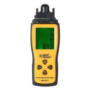
เครื่องวัดแก๊ส (Gas detector)
การตรวจจับแก๊สเป็นส่วนสำคัญของความปลอดภัยเชิงพาณิชย์และอุตสาหกรรม ติดต่อสอบถามได้ที่ บริษัท นีโอนิคส์ จำกัด โทร: 098-479-5684 หรือ 061-8268939 หรือ Line ID:@neonics หรือ Email: sale@tools.in.th
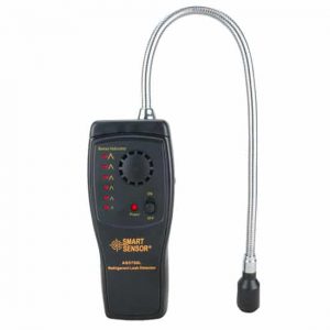
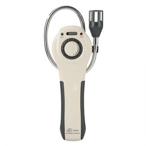
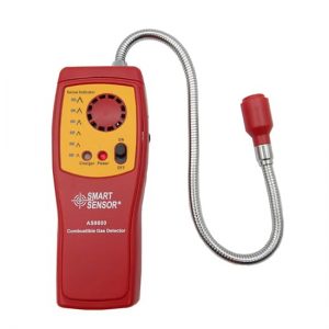
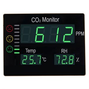
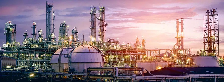
เครื่องตรวจจับก๊าซเป็นเครื่องมือที่มีความซับซ้อนสูงซึ่งวัดหรือตรวจสอบก๊าซตั้งแต่หนึ่งชนิดขึ้นไปภายในพื้นที่ ออกแบบมาเพื่อตรวจจับก๊าซที่ติดไฟได้ ก๊าซพิษ และการสูญเสียออกซิเจน เครื่องตรวจจับก๊าซมักจะเป็นส่วนหนึ่งของระบบความปลอดภัย และโดยทั่วไปแล้วจะนำไปใช้ในพื้นที่จำกัดหรือในพื้นที่อื่นๆ ที่อันตรายจากก๊าซอาจนำไปสู่การสัมผัสสารพิษหรือความเสี่ยงจากไฟไหม้
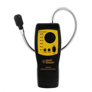
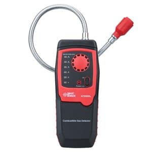
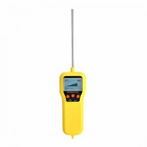
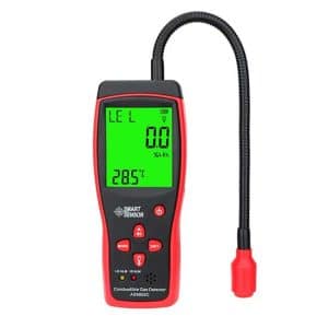
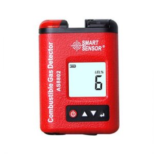
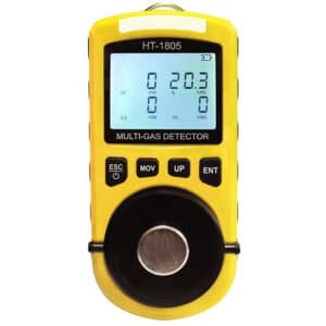
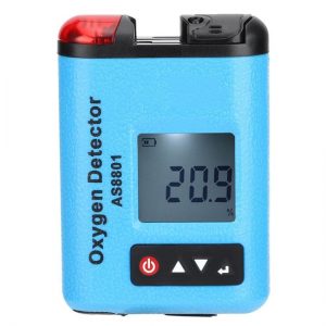
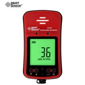
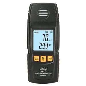
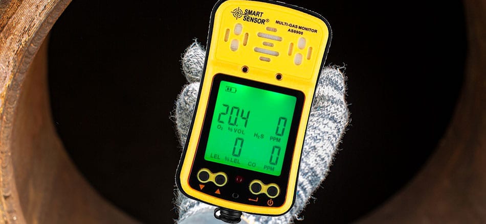
มีทั้งแบบแบบพกพาหรือแบบตายตัว เครื่องตรวจจับก๊าซแบบพกพาถูกใช้เป็นอุปกรณ์ความปลอดภัยส่วนบุคคลและสวมใส่บนเสื้อผ้าหรือบนเข็มขัด/สายรัดเมื่อเข้าสู่พื้นที่จำกัดหรือสภาพแวดล้อมที่เป็นอันตรายอื่นๆ.. อุปกรณ์เหล่านี้มักจะส่งเสียงเตือนเมื่อตรวจพบก๊าซเป้าหมายทำให้ผู้สวมใส่มีโอกาสออกไปได้อย่างปลอดภัย พื้นที่.
เทคโนโลยีการตรวจจับก๊าซมีการพัฒนาอย่างต่อเนื่อง ในปัจจุบันไม่เพียงแต่มีเทคโนโลยีการตรวจจับที่ดีขึ้นเท่านั้น แต่ยังติดตั้งเทคโนโลยีไร้สายที่จะช่วยให้คนทำงานในอนาคต ทำให้ผู้คนปลอดภัยและมีประสิทธิผลมากขึ้น
ประโยชน์ของเครื่องตรวจจับก๊าซแบบพกพาและส่วนบุคคล
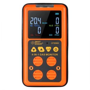
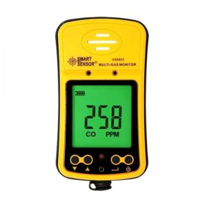
สินค้าแบบพกพาและส่วนบุคคลของเราได้รับความไว้วางใจจากอุตสาหกรรม เราขอเสนอเครื่องตรวจวัดก๊าซที่เหมาะสมกับการใช้งานด้านความปลอดภัยแต่ละแบบ ไม่ว่าจะเป็นสำหรับการตรวจสอบก๊าซแบบเดี่ยวหรือหลายชนิด
- การตรวจจับที่รวดเร็วและเชื่อถือได้จากความเสี่ยงของก๊าซพิษและก๊าซไวไฟ
- จอภาพขนาดกะทัดรัดและน้ำหนักเบาสำหรับแบบหนีบหรือคาดเข็มขัดพร้อมเสียงเตือน ภาพและเสียงเตือนแบบสั่น
- ใช้งานง่ายด้วยปุ่มเดียวและระดับการเตือนที่ตั้งไว้ล่วงหน้า
- ง่ายต่อการบำรุงรักษา ตัวเลือกการบริการและการสอบเทียบ การเคลื่อนตัวของเซ็นเซอร์ต่ำ อายุการใช้งานแบตเตอรี่ที่ยาวนานขึ้น และเซ็นเซอร์ที่มีอายุการใช้งานยาวนานทำให้มีการบำรุงรักษาต่ำ
- ข้อมูลในตัวและความสามารถในการบันทึกเหตุการณ์ช่วยลดภาระของผู้ควบคุมโรงงาน
สอบถามข้อมูล สั่งซื้อ ขอใบเสนอราคา